Quick filters:
Silicon microscope Stock Photos and Images
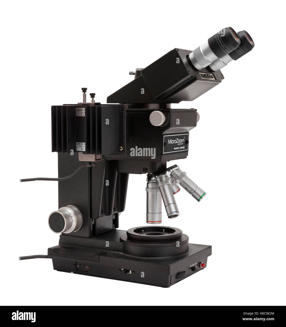 Bausch & Lomb Microzoom compound microscope, used extensively in the semi conductor industry for silicon wafer inspection. Stock Photohttps://www.alamy.com/image-license-details/?v=1https://www.alamy.com/stock-photo-bausch-lomb-microzoom-compound-microscope-used-extensively-in-the-124443612.html
RMH6CW2M–Bausch & Lomb Microzoom compound microscope, used extensively in the semi conductor industry for silicon wafer inspection.
RFB714HT–Silicon atoms of a silicon chip imaged with a scanning tunneling microscope
RF2X3CEG9–Semiconductor Silicon Wafer Probe testing process. 3D rendering image.
RMA47FKY–Atomic Force microscope cantalever scanning over patterned silicon micro electronic thin film devices at high magnification
RF2WB1TC8–Semiconductor silicon wafer defect inspection. Automated optical inspection equipment for semiconductor silicon wafer defects detection. Selective foc
RFE0AC9M–SEM image of SiO2 Silicon Dioxide empty balls, coated with gold and imaged in scanning electron microscope
RF2FMRPH5–Semiconductor silicon wafer under test on the probe station. Selective focus.
RM2AYFRR8–surface of a microchip, Differential interference contrast picture, silicon wafer
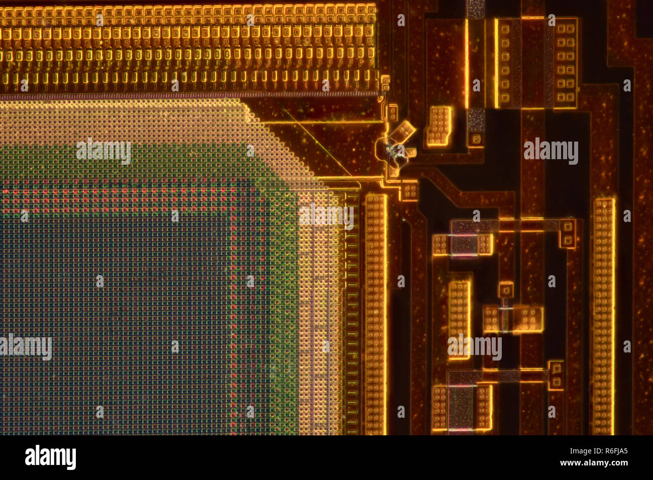 Extreme magnification - Camera sensor under the microscope Stock Photohttps://www.alamy.com/image-license-details/?v=1https://www.alamy.com/extreme-magnification-camera-sensor-under-the-microscope-image227766397.html
RFR6FJA5–Extreme magnification - Camera sensor under the microscope
RF2T8D5DX–silicone wafer under the microscope
RFMNN37R–Illustration of a new technique to eke more power out of solar cells. Owing to physical limits, the maximum amount of sunlight falling on a solar cell that can be converted to electricity is only 34 percent. However, researchers at Warwick University in the UK have demonstrated how this might be overcome, boosting the efficiency of solar cell materials. They pressed the conductive tip of an atomic force microscope into the material, which squeezed and deformed individual crystals of strontium titanate (SrTiO3), titanium dioxide (TiO2), and silicon (Si).
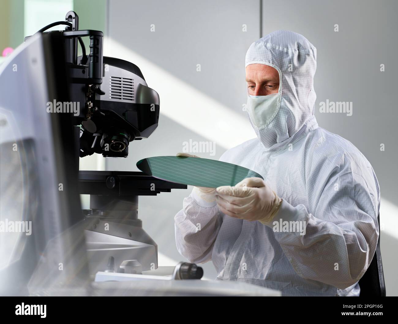 Engineer putting wafer chip on microscope in laboratory Stock Photohttps://www.alamy.com/image-license-details/?v=1https://www.alamy.com/engineer-putting-wafer-chip-on-microscope-in-laboratory-image543839816.html
RF2PGP16G–Engineer putting wafer chip on microscope in laboratory
RFJ4JPJF–Nanostructures on silicon. Coloured scanning electron micrograph (SEM) of nanostructures formed on a silicon surface by a laser beam. This research involves the use of lasers to etch and ablate metal and semiconductor surfaces. The resulting nanostructure
RF2B395DC–Silicon wafer on machine process examining in microscope.
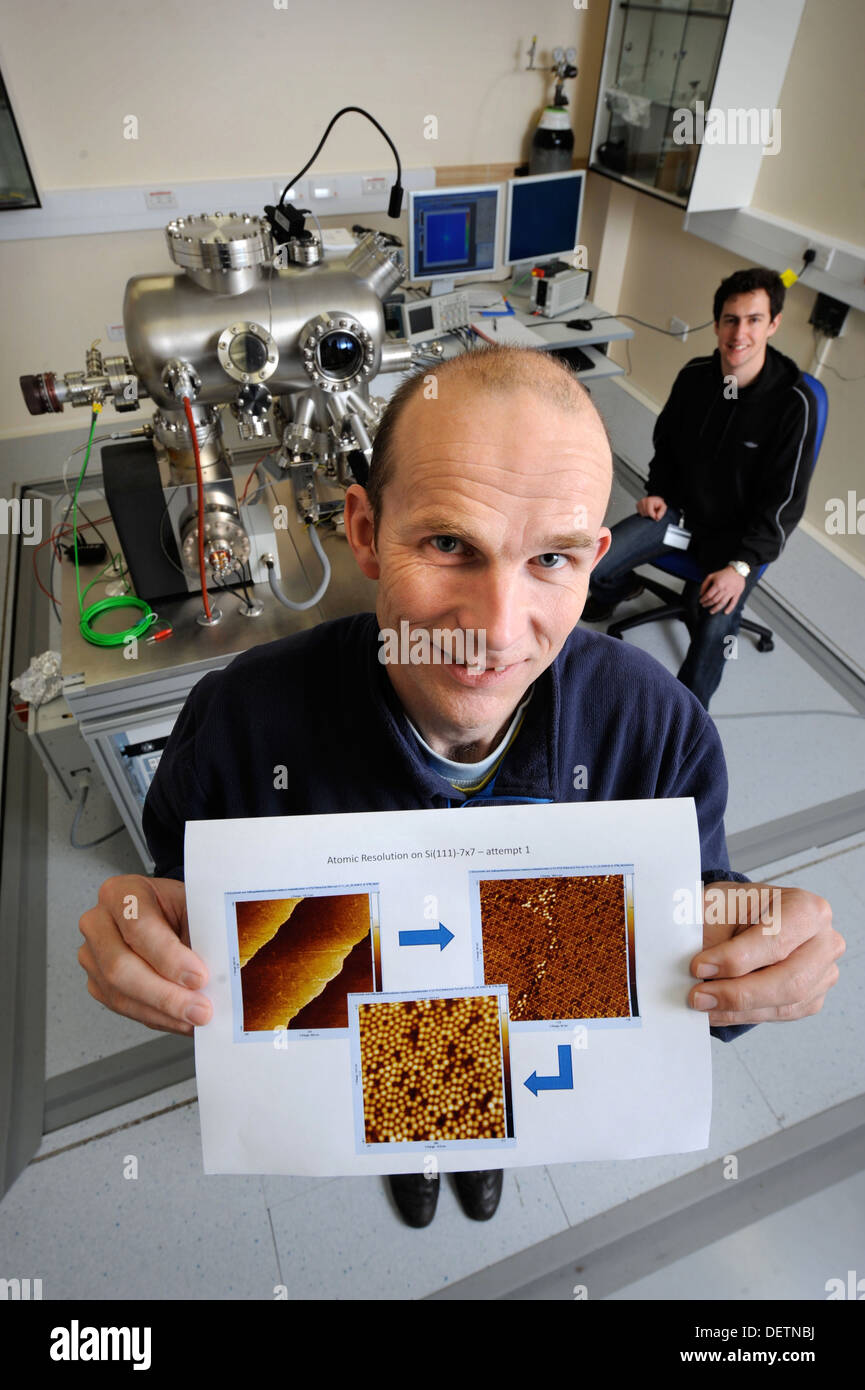 Dr Neil Fox with images showing three levels of magnification of atoms on a sample of silicon produced from a scanning probe mic Stock Photohttps://www.alamy.com/image-license-details/?v=1https://www.alamy.com/dr-neil-fox-with-images-showing-three-levels-of-magnification-of-atoms-image60779926.html
RMDETNBJ–Dr Neil Fox with images showing three levels of magnification of atoms on a sample of silicon produced from a scanning probe mic
RFRDCWXY–Inspection of the quality of silicon chips in the laboratory with a microscope
RMB3RYWK–close up of an Intel Pentium microprocessor silicon chip
 Effects of polarization on crystallization of chmemical substaces as show under the microscope Stock Photohttps://www.alamy.com/image-license-details/?v=1https://www.alamy.com/effects-of-polarization-on-crystallization-of-chmemical-substaces-as-show-under-the-microscope-image558850479.html
RF2RD5RDK–Effects of polarization on crystallization of chmemical substaces as show under the microscope
RM2PNG4T9–Itzehoe, Germany. 04th Apr, 2023. An employee in the production of wafers works under yellow light at a microscope for quality control in the clean room of the semiconductor company Vishay Siliconix Itzehoe GmbH. Wafers are silicon wafers that serve as carriers for the production of microchips. Credit: Christian Charisius/dpa/Alamy Live News
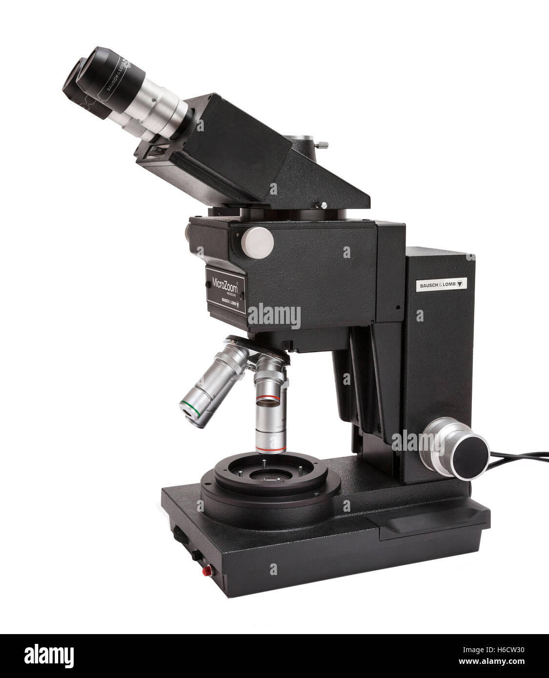 Bausch & Lomb Microzoom compound microscope, used extensively in the semi conductor industry for silicon wafer inspection. Stock Photohttps://www.alamy.com/image-license-details/?v=1https://www.alamy.com/stock-photo-bausch-lomb-microzoom-compound-microscope-used-extensively-in-the-124443620.html
RMH6CW30–Bausch & Lomb Microzoom compound microscope, used extensively in the semi conductor industry for silicon wafer inspection.
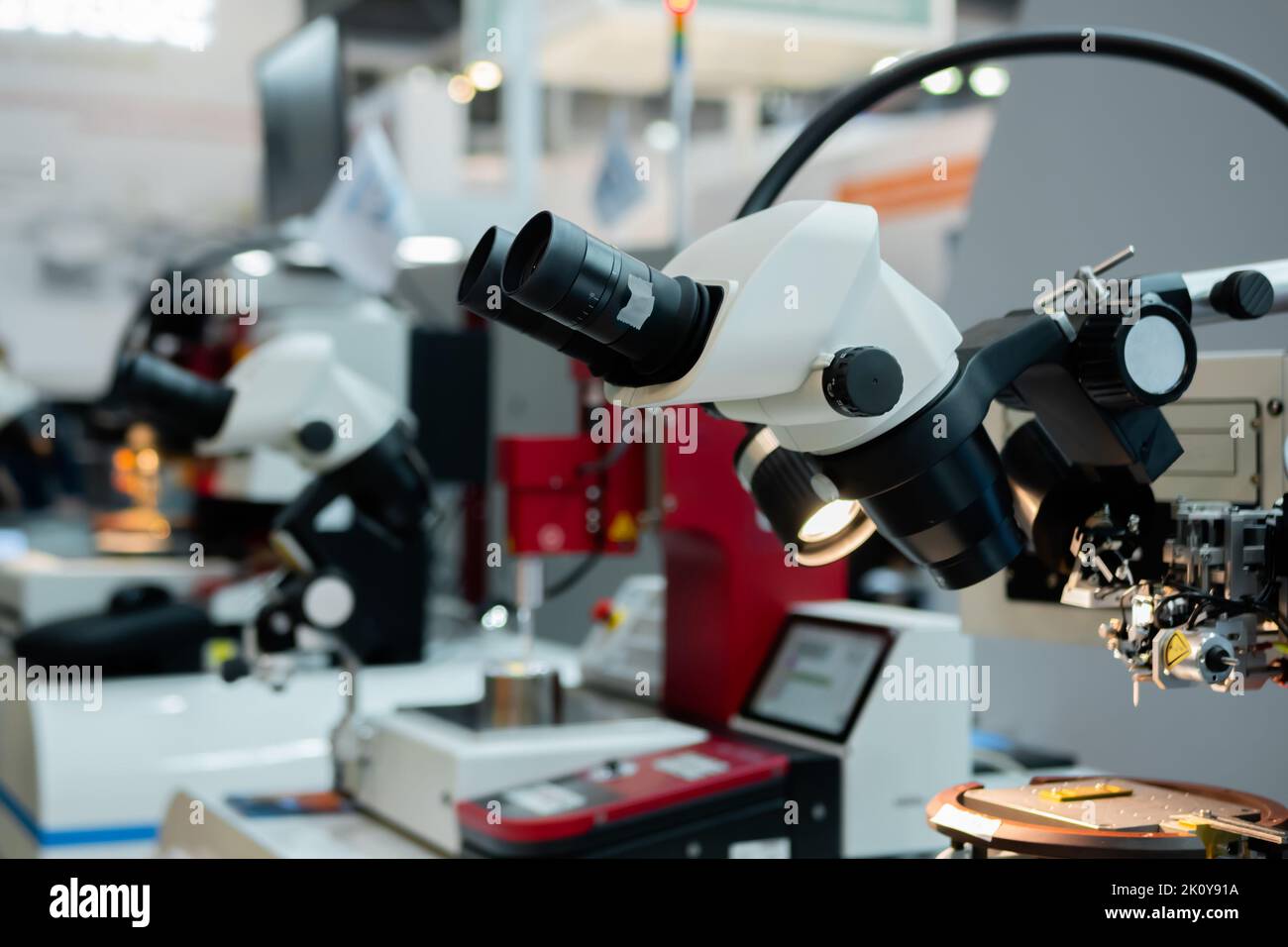 Professional medical microscope in science lab, exhibition Stock Photohttps://www.alamy.com/image-license-details/?v=1https://www.alamy.com/professional-medical-microscope-in-science-lab-exhibition-image482490102.html
RF2K0Y91A–Professional medical microscope in science lab, exhibition
RF2X3CEHT–Clay rendering of Semiconductor Silicon Wafer Probe testing process. 3D rendering image.
RMA47FMJ–Atomic Force microscope cantalever scanning over patterned silicon micro electronic thin film devices at high magnification, UK
 Close-up of the Engineer/ Technician/ Scientist Checking Component under the Microscope. He Wears Sterile Coverall Suit and Protective Glasses Stock Photohttps://www.alamy.com/image-license-details/?v=1https://www.alamy.com/stock-photo-close-up-of-the-engineer-technician-scientist-checking-component-under-176614371.html
RFM79DC3–Close-up of the Engineer/ Technician/ Scientist Checking Component under the Microscope. He Wears Sterile Coverall Suit and Protective Glasses
RF2TBN1HY–silicone wafer under the microscope
RF2FNRK68–Silicon semiconductor wafer on RF probe station. Selective focus.
RM2AYR3MF–surface of a microchip, Differential interference contrast picture, silicon wafer
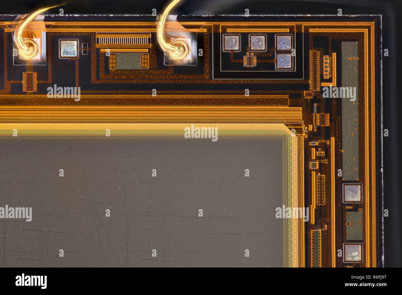 Extreme magnification - Camera sensor under the microscope Stock Photohttps://www.alamy.com/image-license-details/?v=1https://www.alamy.com/extreme-magnification-camera-sensor-under-the-microscope-image227766388.html
RFR6FJ9T–Extreme magnification - Camera sensor under the microscope
RM2AYM9F1–surface of a microchip, Differential interference contrast picture, silicon wafer
RFW3E9D5–Manual probe system for RF test of semiconductor silicon wafers. Selective focus.
RM2B05DRT–surface of a microchip, Differential interference contrast picture, silicon wafer
RF2PGP16R–Engineer checking silicon wafer chip using semiconductor in laboratory
RFJ4JPJY–Nanostructures on silicon. Coloured scanning electron micrograph (SEM) of nanostructures formed on a silicon surface by a laser beam. This research involves the use of lasers to etch and ablate metal and semiconductor surfaces. The resulting nanostructure
RF2B395D5–Silicon wafer on machine process examining in microscope.
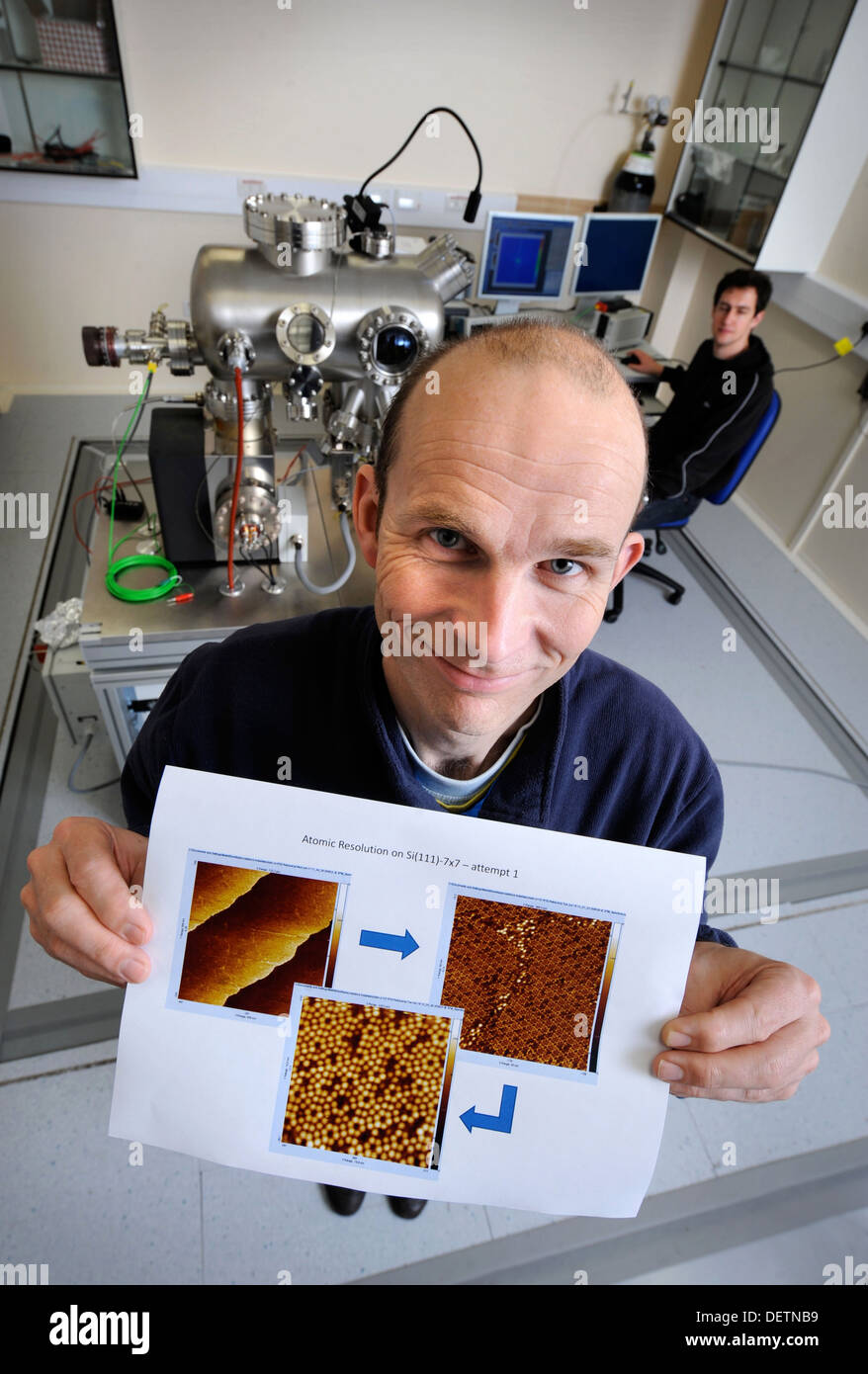 Dr Neil Fox with images showing three levels of magnification of atoms on a sample of silicon produced from a scanning probe mic Stock Photohttps://www.alamy.com/image-license-details/?v=1https://www.alamy.com/dr-neil-fox-with-images-showing-three-levels-of-magnification-of-atoms-image60779917.html
RMDETNB9–Dr Neil Fox with images showing three levels of magnification of atoms on a sample of silicon produced from a scanning probe mic
RFRHPNT5–Inspection of the quality of silicon chips in the laboratory with a microscope
RMB3T0CY–close up of an Intel Pentium microprocessor silicon chip
 Effects of polarization on crystallization of chmemical substaces as show under the microscope Stock Photohttps://www.alamy.com/image-license-details/?v=1https://www.alamy.com/effects-of-polarization-on-crystallization-of-chmemical-substaces-as-show-under-the-microscope-image558850506.html
RF2RD5REJ–Effects of polarization on crystallization of chmemical substaces as show under the microscope
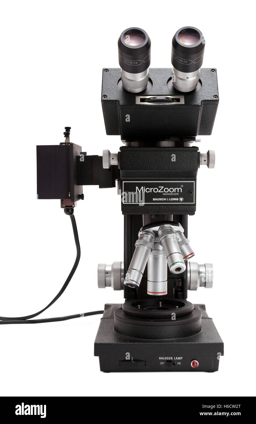 Bausch & Lomb Microzoom compound microscope, used extensively in the semi conductor industry for silicon wafer inspection. Stock Photohttps://www.alamy.com/image-license-details/?v=1https://www.alamy.com/stock-photo-bausch-lomb-microzoom-compound-microscope-used-extensively-in-the-124443616.html
RMH6CW2T–Bausch & Lomb Microzoom compound microscope, used extensively in the semi conductor industry for silicon wafer inspection.
RM2PNG4T6–Itzehoe, Germany. 04th Apr, 2023. An employee in the production of wafers works under yellow light at a microscope for quality control in the clean room of the semiconductor company Vishay Siliconix Itzehoe GmbH. Wafers are silicon wafers that serve as carriers for the production of microchips. Credit: Christian Charisius/dpa/Alamy Live News
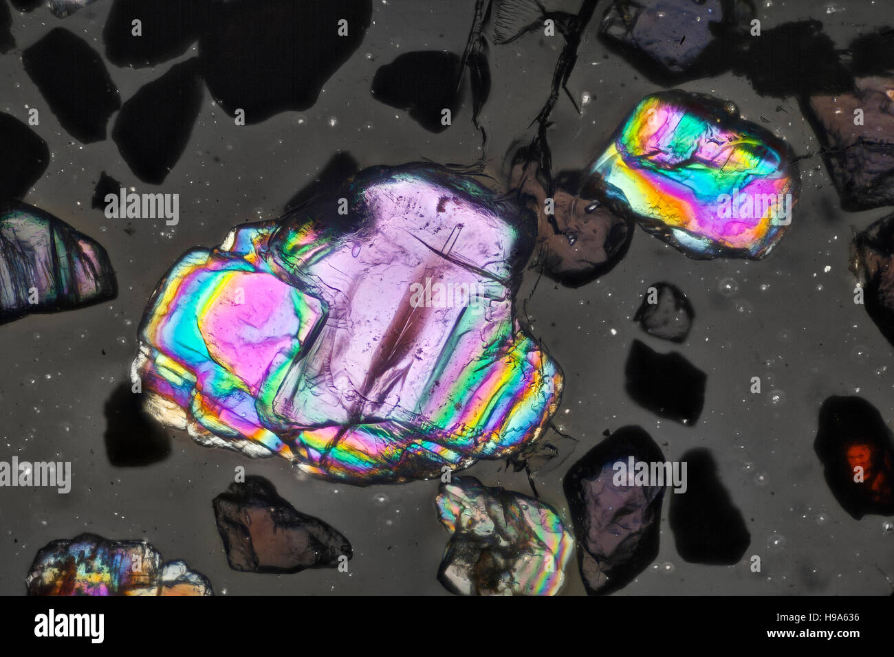 Sand with Cassiterite & Columbite, polarized photomicrograph Stock Photohttps://www.alamy.com/image-license-details/?v=1https://www.alamy.com/stock-photo-sand-with-cassiterite-columbite-polarized-photomicrograph-126228794.html
RMH9A636–Sand with Cassiterite & Columbite, polarized photomicrograph
 Composite of image showing cantalever scanning thin film devices while using Atomic Force microscope at high resolution Stock Photohttps://www.alamy.com/image-license-details/?v=1https://www.alamy.com/stock-photo-composite-of-image-showing-cantalever-scanning-thin-film-devices-while-10959323.html
RMA47FKT–Composite of image showing cantalever scanning thin film devices while using Atomic Force microscope at high resolution
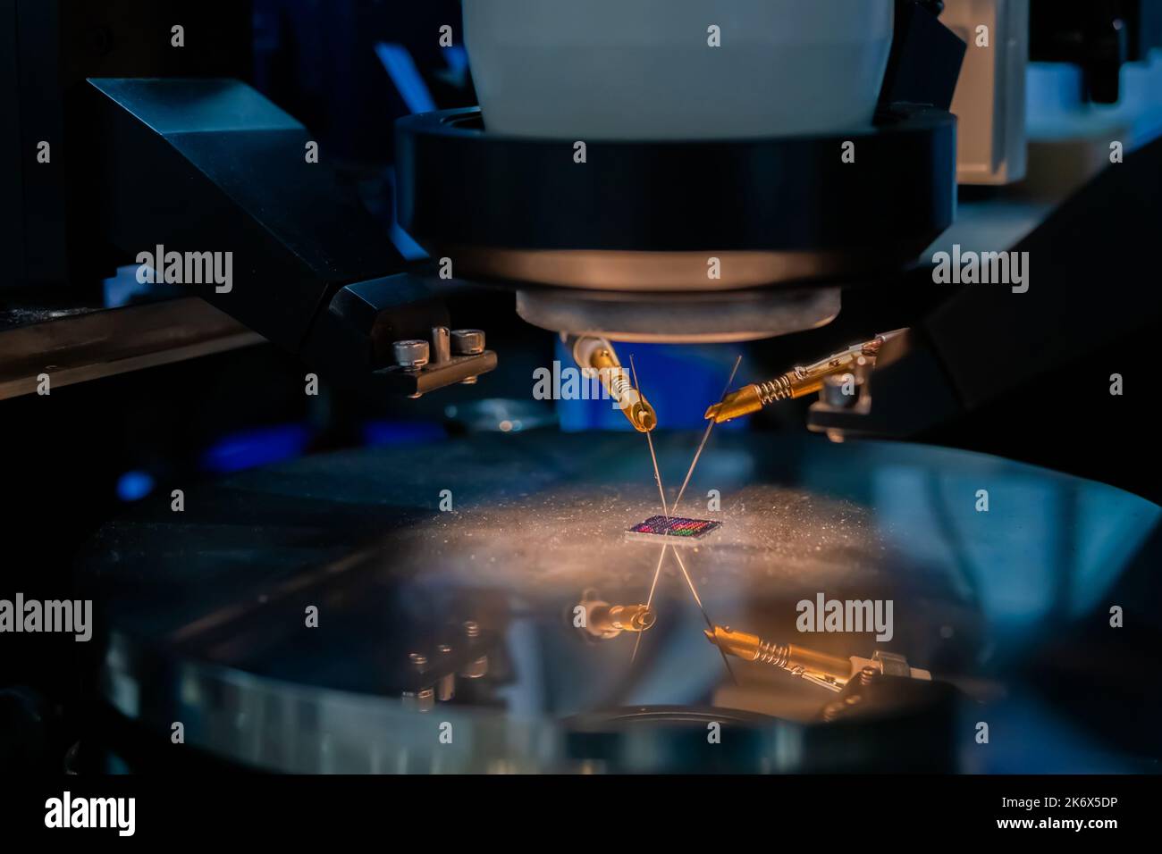 Professional medical microscope in science lab, exhibition Stock Photohttps://www.alamy.com/image-license-details/?v=1https://www.alamy.com/professional-medical-microscope-in-science-lab-exhibition-image486153298.html
RF2K6X5DP–Professional medical microscope in science lab, exhibition
 Electronics Factory Worker in White Work Coat Inspects a Printed Circuit Board Through a Digital Microscope. High Tech Factory Facility. Stock Photohttps://www.alamy.com/image-license-details/?v=1https://www.alamy.com/electronics-factory-worker-in-white-work-coat-inspects-a-printed-circuit-board-through-a-digital-microscope-high-tech-factory-facility-image382738777.html
RF2D6K761–Electronics Factory Worker in White Work Coat Inspects a Printed Circuit Board Through a Digital Microscope. High Tech Factory Facility.
RF2T8D5E5–silicone wafer under the microscope
 Technician examining chip, using microscope to run diagnosis and upgrade device Stock Photohttps://www.alamy.com/image-license-details/?v=1https://www.alamy.com/technician-examining-chip-using-microscope-to-run-diagnosis-and-upgrade-device-image339886877.html
RF2AMY551–Technician examining chip, using microscope to run diagnosis and upgrade device
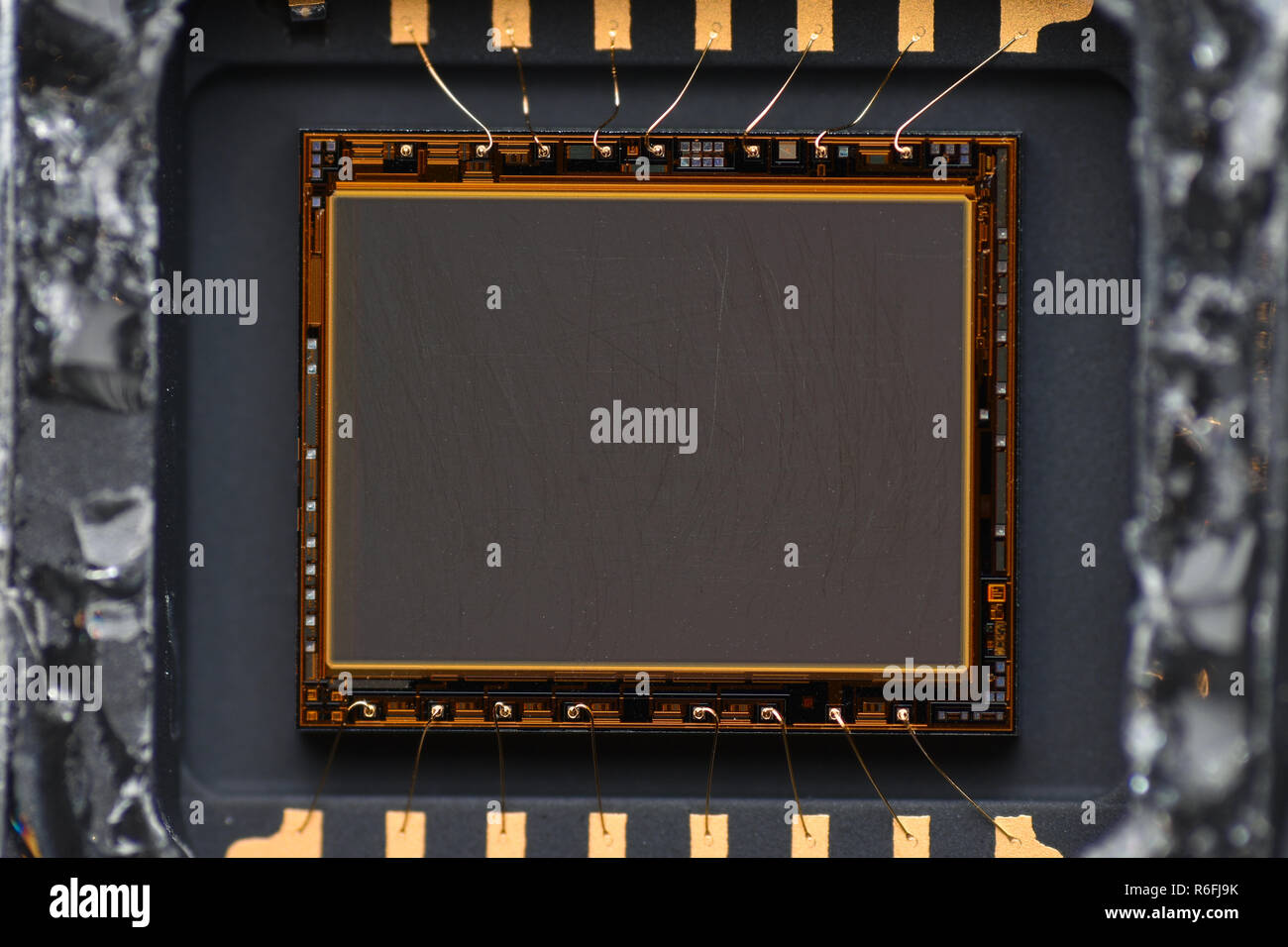 Extreme magnification - Camera sensor under the microscope Stock Photohttps://www.alamy.com/image-license-details/?v=1https://www.alamy.com/extreme-magnification-camera-sensor-under-the-microscope-image227766383.html
RFR6FJ9K–Extreme magnification - Camera sensor under the microscope
RF2WG3YFM–Microcones on silicon, SEM
RFKM71G6–Semiconductor silicon wafer undergoing probe testing. Selective focus.
RM2AYYJ3E–surface of a microchip, Differential interference contrast picture, silicon wafer
RF2C49AW9–Silicon on the periodic table of elements
 Drops from a pipette. Liquid gel or serum on a microscope screen on a white background Stock Photohttps://www.alamy.com/image-license-details/?v=1https://www.alamy.com/drops-from-a-pipette-liquid-gel-or-serum-on-a-microscope-screen-on-a-white-background-image447903060.html
RF2H0KMWT–Drops from a pipette. Liquid gel or serum on a microscope screen on a white background
RF2B395PY–Silicon wafer on machine process examining in microscope.
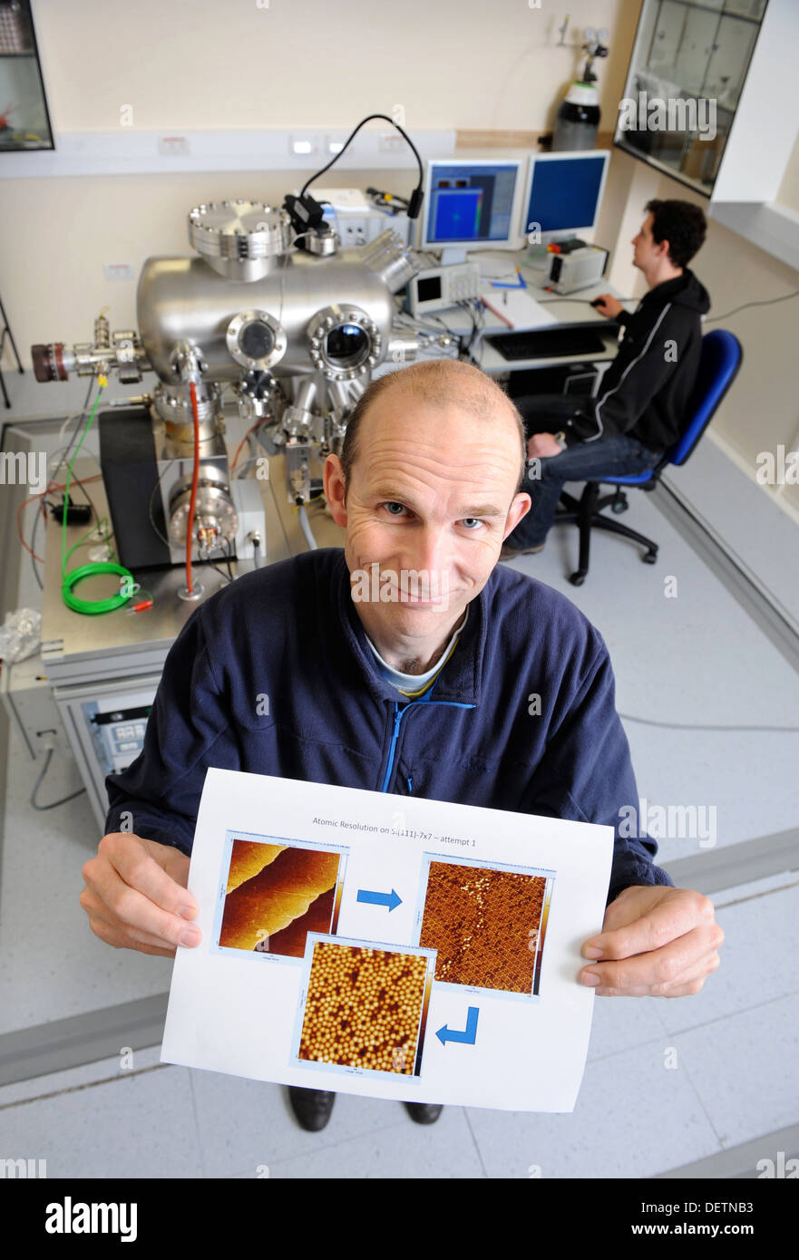 Dr Neil Fox with images showing three levels of magnification of atoms on a sample of silicon produced from a scanning probe mic Stock Photohttps://www.alamy.com/image-license-details/?v=1https://www.alamy.com/dr-neil-fox-with-images-showing-three-levels-of-magnification-of-atoms-image60779911.html
RMDETNB3–Dr Neil Fox with images showing three levels of magnification of atoms on a sample of silicon produced from a scanning probe mic
RF2B38Y72–Checking microchips on silicon wafer with probe station and microscope.Microelecronics.
RFRG30WH–Inspection of the quality of silicon chips in the laboratory with a microscope
RF2B395DF–Silicon wafer on machine process examining in microscope.
RFEGT5NG–silicon crystal with photovoltaic cells in the hand of the scientist
RM2PNG449–Itzehoe, Germany. 04th Apr, 2023. An employee in the production of wafers works under yellow light at a microscope for quality control in the clean room of the semiconductor company Vishay Siliconix Itzehoe GmbH. Wafers are silicon wafers that serve as carriers for the production of microchips. Credit: Christian Charisius/dpa/Alamy Live News
 Sand with Cassiterite & Columbite, polarized photomicrograph Stock Photohttps://www.alamy.com/image-license-details/?v=1https://www.alamy.com/stock-photo-sand-with-cassiterite-columbite-polarized-photomicrograph-126228790.html
RMH9A632–Sand with Cassiterite & Columbite, polarized photomicrograph
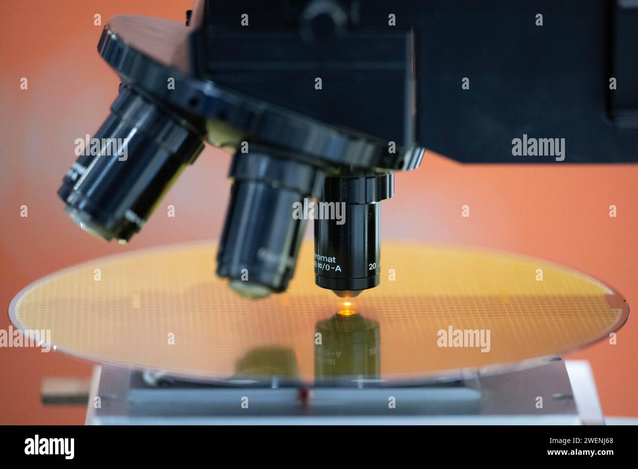 Dresden, Germany. 19th Jan, 2024. A wafer from the X-FAB Group lies under a microscope at the 'KarriereStart' job fair. Credit: Sebastian Kahnert/dpa/Alamy Live News Stock Photohttps://www.alamy.com/image-license-details/?v=1https://www.alamy.com/dresden-germany-19th-jan-2024-a-wafer-from-the-x-fab-group-lies-under-a-microscope-at-the-karrierestart-job-fair-credit-sebastian-kahnertdpaalamy-live-news-image594232976.html
RM2WENJ68–Dresden, Germany. 19th Jan, 2024. A wafer from the X-FAB Group lies under a microscope at the 'KarriereStart' job fair. Credit: Sebastian Kahnert/dpa/Alamy Live News
 Effects of polarization on crystallization of chmemical substaces as show under the microscope Stock Photohttps://www.alamy.com/image-license-details/?v=1https://www.alamy.com/effects-of-polarization-on-crystallization-of-chmemical-substaces-as-show-under-the-microscope-image558850206.html
RF2RD5R3X–Effects of polarization on crystallization of chmemical substaces as show under the microscope
 Electronics Factory Worker in White Work Coat is Soldering a Printed Circuit Board Through a Digital Microscope. High Tech Factory Facility. Stock Photohttps://www.alamy.com/image-license-details/?v=1https://www.alamy.com/electronics-factory-worker-in-white-work-coat-is-soldering-a-printed-circuit-board-through-a-digital-microscope-high-tech-factory-facility-image382738780.html
RF2D6K764–Electronics Factory Worker in White Work Coat is Soldering a Printed Circuit Board Through a Digital Microscope. High Tech Factory Facility.
RF2T8D4CF–silicone wafer under the microscope
 Silica gel for moisture control, absorbent particles under a light microscope, magnification 40 times Stock Photohttps://www.alamy.com/image-license-details/?v=1https://www.alamy.com/silica-gel-for-moisture-control-absorbent-particles-under-a-light-microscope-magnification-40-times-image456078012.html
RF2HE044C–Silica gel for moisture control, absorbent particles under a light microscope, magnification 40 times
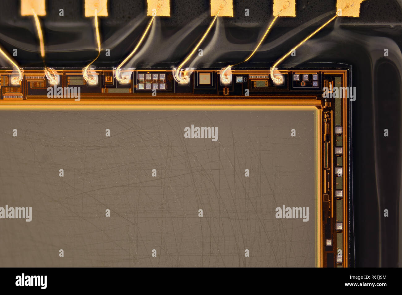 Extreme magnification - Camera sensor under the microscope Stock Photohttps://www.alamy.com/image-license-details/?v=1https://www.alamy.com/extreme-magnification-camera-sensor-under-the-microscope-image227766384.html
RFR6FJ9M–Extreme magnification - Camera sensor under the microscope
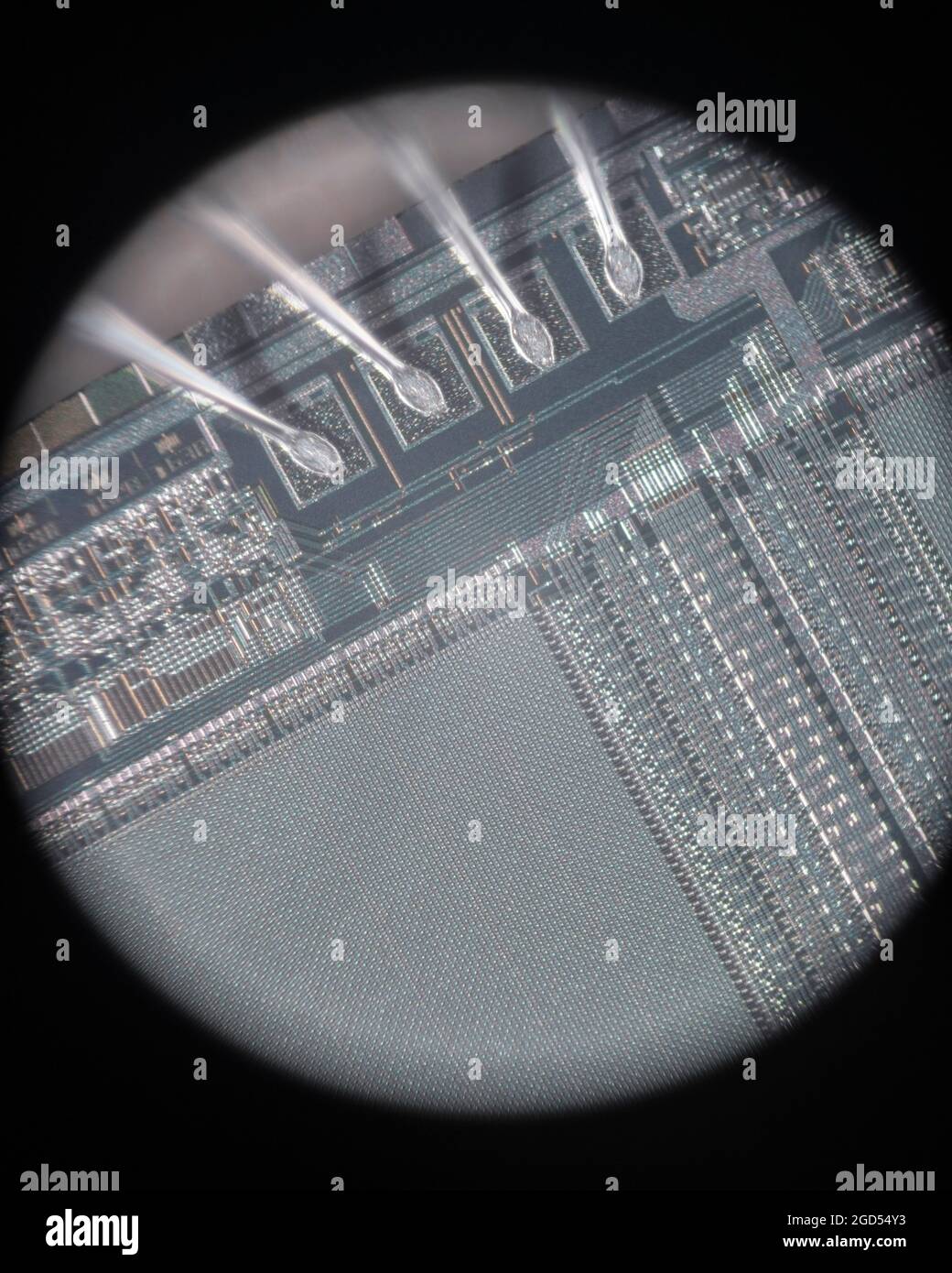 Microphotograph of internal wiring and die of Texas Instruments TMS 2532A-45JL UV eprom. Taken through a 10x standard microscope objective. SEE NOTES Stock Photohttps://www.alamy.com/image-license-details/?v=1https://www.alamy.com/microphotograph-of-internal-wiring-and-die-of-texas-instruments-tms-2532a-45jl-uv-eprom-taken-through-a-10x-standard-microscope-objective-see-notes-image438363383.html
RM2GD54Y3–Microphotograph of internal wiring and die of Texas Instruments TMS 2532A-45JL UV eprom. Taken through a 10x standard microscope objective. SEE NOTES
 Engineer sitting in robot fabrication room use measuring microscope machine check microchip Stock Photohttps://www.alamy.com/image-license-details/?v=1https://www.alamy.com/engineer-sitting-in-robot-fabrication-room-use-measuring-microscope-machine-check-microchip-image504140528.html
RF2M85GAT–Engineer sitting in robot fabrication room use measuring microscope machine check microchip
RM2B05DKD–surface of a microchip, Differential interference contrast picture, silicon wafer
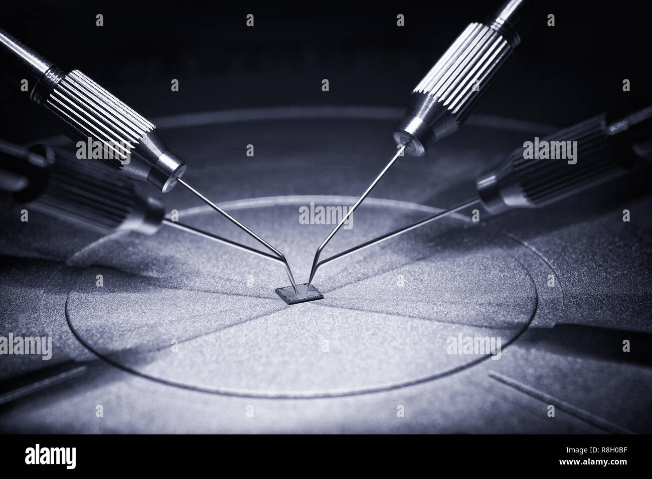 manufacture of chips on a printed circuit board under a microscope Stock Photohttps://www.alamy.com/image-license-details/?v=1https://www.alamy.com/manufacture-of-chips-on-a-printed-circuit-board-under-a-microscope-image229025539.html
RFR8H0BF–manufacture of chips on a printed circuit board under a microscope
 Drops from a pipette. Liquid gel or serum on a microscope screen on a white background Stock Photohttps://www.alamy.com/image-license-details/?v=1https://www.alamy.com/drops-from-a-pipette-liquid-gel-or-serum-on-a-microscope-screen-on-a-white-background-image449646762.html
RF2H3F50X–Drops from a pipette. Liquid gel or serum on a microscope screen on a white background
 Close up of examining of test sample of microchip transistor under the microscope in laboratory. Equipment for testing microchips. Automation of produ Stock Photohttps://www.alamy.com/image-license-details/?v=1https://www.alamy.com/close-up-of-examining-of-test-sample-of-microchip-transistor-under-the-microscope-in-laboratory-equipment-for-testing-microchips-automation-of-produ-image561255577.html
RF2RH3B61–Close up of examining of test sample of microchip transistor under the microscope in laboratory. Equipment for testing microchips. Automation of produ
 Technician in a clean room environment using a microscope to inspect computer semi conductors Stock Photohttps://www.alamy.com/image-license-details/?v=1https://www.alamy.com/stock-photo-technician-in-a-clean-room-environment-using-a-microscope-to-inspect-35088695.html
RMC12BYK–Technician in a clean room environment using a microscope to inspect computer semi conductors
 Close up of examining of test sample of microchip transistor under the microscope in laboratory. Equipment for testing microchips. Automation of produ Stock Photohttps://www.alamy.com/image-license-details/?v=1https://www.alamy.com/close-up-of-examining-of-test-sample-of-microchip-transistor-under-the-microscope-in-laboratory-equipment-for-testing-microchips-automation-of-produ-image418582776.html
RF2F902GT–Close up of examining of test sample of microchip transistor under the microscope in laboratory. Equipment for testing microchips. Automation of produ
RFB71199–Silicon atoms of a silicon chip imaged with a scanning tunneling microscope
RF2B395RB–Silicon wafer on machine process examining in microscope.
RFGF845P–silicon crystal with photovoltaic cells in the hand of the scientist
RMHRJKC0–Silicon Solar Cell, LM
 Sand with Cassiterite & Columbite, polarized photomicrograph Stock Photohttps://www.alamy.com/image-license-details/?v=1https://www.alamy.com/stock-photo-sand-with-cassiterite-columbite-polarized-photomicrograph-126228801.html
RMH9A63D–Sand with Cassiterite & Columbite, polarized photomicrograph
RFRADAWD–Inspection of the quality of silicon chips in the laboratory with a microscope
 Effects of polarization on crystallization of chmemical substaces as show under the microscope Stock Photohttps://www.alamy.com/image-license-details/?v=1https://www.alamy.com/effects-of-polarization-on-crystallization-of-chmemical-substaces-as-show-under-the-microscope-image558850110.html
RF2RD5R0E–Effects of polarization on crystallization of chmemical substaces as show under the microscope
 Electronics Factory Worker in White Work Coat is Soldering a Printed Circuit Board Through a Digital Microscope. High Tech Factory Facility. Stock Photohttps://www.alamy.com/image-license-details/?v=1https://www.alamy.com/electronics-factory-worker-in-white-work-coat-is-soldering-a-printed-circuit-board-through-a-digital-microscope-high-tech-factory-facility-image382738854.html
RF2D6K78P–Electronics Factory Worker in White Work Coat is Soldering a Printed Circuit Board Through a Digital Microscope. High Tech Factory Facility.
RF2T8D3P7–silicone wafer under the microscope
 Silica gel for moisture control, absorbent particles under a light microscope, magnification 40 times Stock Photohttps://www.alamy.com/image-license-details/?v=1https://www.alamy.com/silica-gel-for-moisture-control-absorbent-particles-under-a-light-microscope-magnification-40-times-image455565662.html
RF2HD4PJ6–Silica gel for moisture control, absorbent particles under a light microscope, magnification 40 times
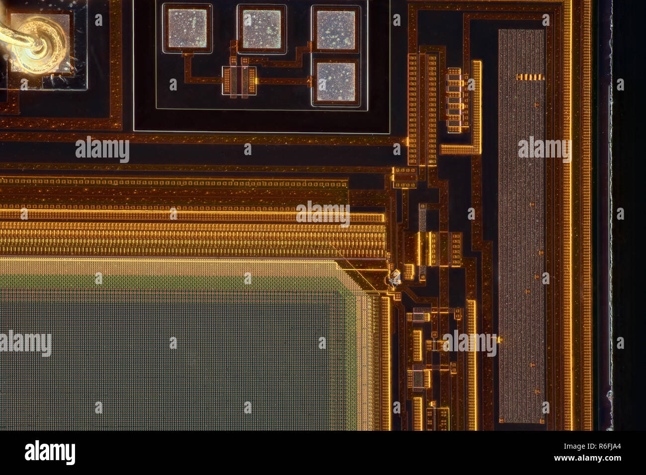 Extreme magnification - Camera sensor under the microscope Stock Photohttps://www.alamy.com/image-license-details/?v=1https://www.alamy.com/extreme-magnification-camera-sensor-under-the-microscope-image227766396.html
RFR6FJA4–Extreme magnification - Camera sensor under the microscope
RF2TBN1AM–silicone wafer under the microscope,integrated circuits to manufacture CPU and GPU
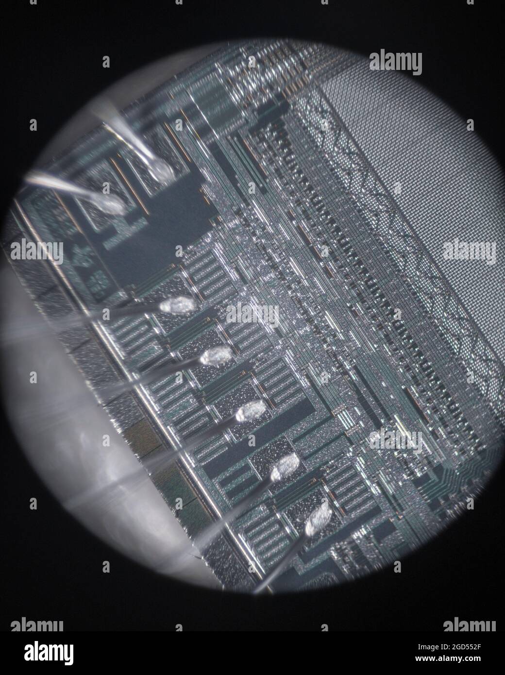 Microphotograph of internal wiring and die of Texas Instruments TMS 2532A-45JL UV eprom. Taken through a 10x standard microscope objective. SEE NOTES Stock Photohttps://www.alamy.com/image-license-details/?v=1https://www.alamy.com/microphotograph-of-internal-wiring-and-die-of-texas-instruments-tms-2532a-45jl-uv-eprom-taken-through-a-10x-standard-microscope-objective-see-notes-image438363479.html
RM2GD552F–Microphotograph of internal wiring and die of Texas Instruments TMS 2532A-45JL UV eprom. Taken through a 10x standard microscope objective. SEE NOTES
RM2AYM9R7–surface of a microchip, Differential interference contrast picture, silicon wafer
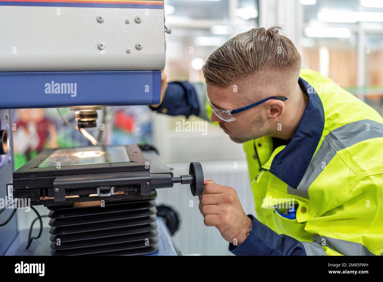 Engineer sitting in robot fabrication room use measuring microscope machine check microchip Stock Photohttps://www.alamy.com/image-license-details/?v=1https://www.alamy.com/engineer-sitting-in-robot-fabrication-room-use-measuring-microscope-machine-check-microchip-image504140157.html
RF2M85FWH–Engineer sitting in robot fabrication room use measuring microscope machine check microchip
 Drops from a pipette. Liquid gel or serum on a microscope screen on a white background Stock Photohttps://www.alamy.com/image-license-details/?v=1https://www.alamy.com/drops-from-a-pipette-liquid-gel-or-serum-on-a-microscope-screen-on-a-white-background-image448824004.html
RF2H25KGM–Drops from a pipette. Liquid gel or serum on a microscope screen on a white background
 Industry Manufacturing Electronics Technician working with microscope Silicon wafer Concept Stock Photohttps://www.alamy.com/image-license-details/?v=1https://www.alamy.com/stock-photo-industry-manufacturing-electronics-technician-working-with-microscope-12177543.html
RMA8W1AG–Industry Manufacturing Electronics Technician working with microscope Silicon wafer Concept
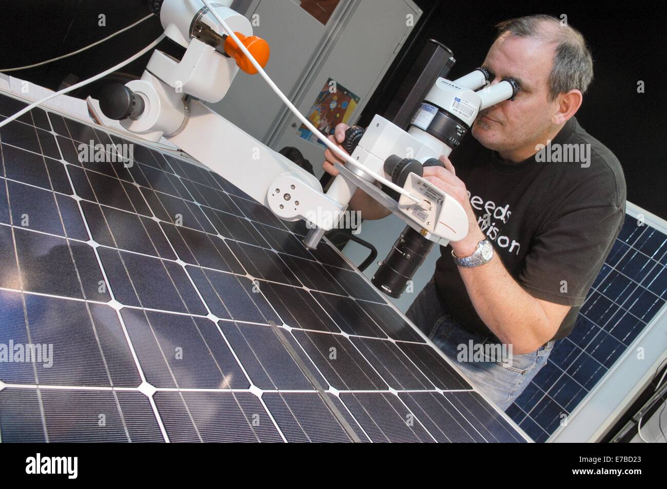 Ispra (Italy), JRC, Joint European Research Center, Institute for the Atmosphere and the sustainability Stock Photohttps://www.alamy.com/image-license-details/?v=1https://www.alamy.com/stock-photo-ispra-italy-jrc-joint-european-research-center-institute-for-the-atmosphere-73395787.html
RME7BD23–Ispra (Italy), JRC, Joint European Research Center, Institute for the Atmosphere and the sustainability
 Close up of examining of test sample of microchip transistor under the microscope in laboratory. Equipment for testing microchips. Automation of produ Stock Photohttps://www.alamy.com/image-license-details/?v=1https://www.alamy.com/close-up-of-examining-of-test-sample-of-microchip-transistor-under-the-microscope-in-laboratory-equipment-for-testing-microchips-automation-of-produ-image418949764.html
RF2F9GPKG–Close up of examining of test sample of microchip transistor under the microscope in laboratory. Equipment for testing microchips. Automation of produ
RF2YK63PX–Silicon (Si 14) pure crystalline form. Specimen from . Micro photography extreme close-up. microscope mineral crystal photography for Scientific use.
RF2B395R5–Silicon wafer on machine process examining in microscope.
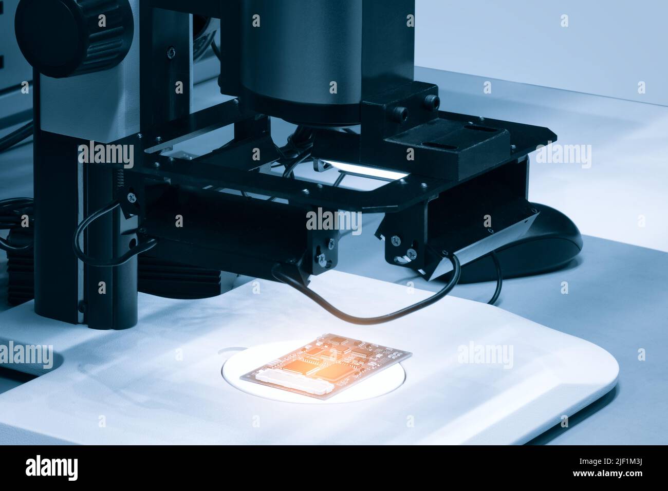 Chip testing equipment. Manufacturing of microchips. A close-up study of a test sample of a transistor chip under a microscope in the laboratory. Auto Stock Photohttps://www.alamy.com/image-license-details/?v=1https://www.alamy.com/chip-testing-equipment-manufacturing-of-microchips-a-close-up-study-of-a-test-sample-of-a-transistor-chip-under-a-microscope-in-the-laboratory-auto-image473937510.html
RF2JF1M3J–Chip testing equipment. Manufacturing of microchips. A close-up study of a test sample of a transistor chip under a microscope in the laboratory. Auto
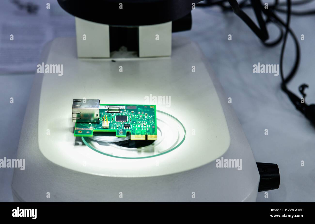 CMM machines for inspection high precision chip components on pcb board during working in industrial Stock Photohttps://www.alamy.com/image-license-details/?v=1https://www.alamy.com/cmm-machines-for-inspection-high-precision-chip-components-on-pcb-board-during-working-in-industrial-image592748871.html
RF2WCA16F–CMM machines for inspection high precision chip components on pcb board during working in industrial
 Sand with Cassiterite & Columbite, polarized photomicrograph Stock Photohttps://www.alamy.com/image-license-details/?v=1https://www.alamy.com/stock-photo-sand-with-cassiterite-columbite-polarized-photomicrograph-126228810.html
RMH9A63P–Sand with Cassiterite & Columbite, polarized photomicrograph
RFT31Y7W–Inspection of the quality of silicon chips in the laboratory with a microscope
 Effects of polarization on crystallization of chmemical substaces as show under the microscope Stock Photohttps://www.alamy.com/image-license-details/?v=1https://www.alamy.com/effects-of-polarization-on-crystallization-of-chmemical-substaces-as-show-under-the-microscope-image558850072.html
RF2RD5PY4–Effects of polarization on crystallization of chmemical substaces as show under the microscope